EECAD Guidelines & Standards
Creating Schematic Symbols
General
- If creating your symbols thru the schematic editor, open a standard setup drawing, such as b_setup.sch. This will ensure you
have the correct fonts available to you when you create your symbol. If you are creating your symbols thru Library Executive,
make sure you are using the following fonts: Pinstyle[1] (which should be True type font Arial 10 pt) and Partstyle[1] (which
should be True Type font Arial 12pt).
- Do not create a new symbol if one currently exists in the master JLAB libraries! You can search the master Altium listing by
going to: \\jlabgrp\eecad\pcad\master libraries\cleaned Altium libraries\ and viewing the file pcad library index.
- Use 5 mil lines for all graphics unless you want something to print bold. In that case use 10 mil lines for those lines you
want bold.
- When drawing a circle, do it using two 180 degree arcs. (Some of the printers don't like circles and will not print them!)
- Use the textstyle of Pinstyle[1] for pin designators and any text inside the outlines of the parts.
- Use the textstyle of Partstyle[1] for RefDes, Value and Type attributes.
- Place the reference point on the uppermost pin on the left hand side of the part.
- Keep in mind the size of your symbol. For example, all op amps should be the same size and discrete components(resistors,
caps, diodes) should never be bigger than a gate.
- As a general rule, all like gates in a package should look the same. For example, if you have a quad op amp all gates should
physically look the same to enable gate swapping. Power pins should either be on a totally separate and unique gate or should
be defined in the .Pins View. of the library manager as to their function. If done the latter way, they can then be shown on
your drawing in a .Power Table. that lists all power & ground connections for ICS.
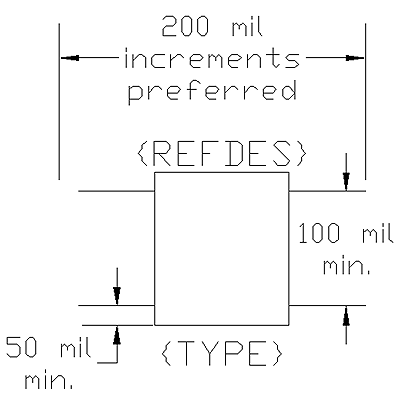
- The overall size of the end of pin to end of pin should be in 100 mil increments with 200 mils being preferred. (See example
below)
Pin Placement
- In general, use short pins. The preferred size is 200 mils, which must be set by selecting PIN LENGTH- USER and entering 200
for the length.
- Be aware of whether or not you want the pin name and number to be visible when selecting the pin. (there are check boxes for
this) In general, resistors, capacitors, etc. do not show pin name or number, connectors, transistors, and ICs do.
- Place pins on a minimum 50 mil grid snap.
- The minimum spacing between pins is 100 mils. For analog ICs, use a minimum 200 mil spacing.
- If mounting holes must be tied to ground (or any other potential), they should have a pin assigned to them. However, this
function MAY be done manually in the PCB editor. You can also use a technique of overlaying pins.(your main pin is 200 mil in
length and you lay one or more pins that are 10 mil in length over it.) Contact Tom Powers or Lori Zukerman for more
information on this technique.
- Remember that the mapping of symbol pins to pattern pins is done in the Library manager. You do not need to assign the pattern
pin numbers to the symbol, only be aware of the order of your pins. Pin numbers must start at one and be sequential , no
skipping numbers. A hint on numbering pins is to enter all of the pins, then select UTILS-Renumber. Check the .pin. option,
then click OK. Now, click on the pins in the order that you want them to be renumbered. (It is a good idea to make them the
same numbers as the pin out of the device, but it may not be possible.)
- If you use a vertical orientation on a pin, please make sure you rotate the pin number and name(if visible) so that it is the
same as all your horizontal pins. You can do this by doing a SHIFT, left mouse click on the object you want rotated.
Return to EECAD Guidelines Home