Pockels Cell DEI driver response tests
John C. Hansknecht
January 2005
Roger Carlini has expressed to the electron gun group a desire to flip polarization at a rate that could be as high as 300 Hz. A dead time of 500 usec would create an unacceptable DAQ loss for the experiment, and I thought I had tried everything with my Behlke switches. Roger pointed out that there are very fast high voltage switches available from Directed Energy, Inc. that were already configured in a “ready to go” chassis. We purchased the switch and I ran a series of tests that yielded some surprising results. Most notably, my efforts in the past to speed up the transition of the high voltage were actually in error. I needed to slow down the high voltage transition in order to critically damp the oscillations that were induced in the crystal.
I had at my disposal a relatively new item that could help me quantify my measurements as being either voltage induced, photo-diode induced, or cell induced phenomenon. The RTP cell is a new (to me) type of Pockel’s cell that has an extremely fast response time and little to no piezo electric resonances. One might think that this would be a candidate cell for helicity reversal, but it has a low extinction ratio (200 :1) vs. the (3000 : 1) typically provided by the KD*P crystal. This produces parity errors beyond the scope of this discussion. By using the RTP cell for my initial measurements I was able to quantify the effects of the high voltage and photo-diode.
The data that follows shows the sequence of the tests performed.
Figure 2
Test 1. Prove that the photo-diode optical response is fast enough for the subsequent tests. RTP cell is used because it is known to have little to no piezo resonance. The DEI switch is rated to switch within 80 nsec with stable output “if” the 1 meter long RG-8 cable provided is utilized.
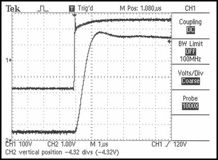
Figure 3
RTP Cell
0 to 790V Switch transition on channel 1
Optical response from photo-diode on channel 2. Note: The cell alignment was not critical for these measurements. The experiment was simply set up to measure a stress induced birefringence change from one voltage state to another. We are only interested in the time it takes for the crystal to change from one stable birefringence state to another stable state.
Result:
Trace proves that photo-diode time response is adequate for the tests. The upper trace is the high voltage as measured from the DEI switch output and the lower trace is the photodiode response from an intensity change on laser light passing through the RTP cell. It also shows that RTP crystal is also quite fast and the high voltage transition shows little overshoot or undershoot.
Note: If your application requires a fast, flat top
slice of laser light, the RTP is your cell.
You will notice in the following tests that KD*P will ring when it is
asked to respond too fast.
Test 2: Apply the same voltage to the RTP cell that would normally be applied to a KD*P cell. Verify system response and prove that there is not a problem with the HV switch
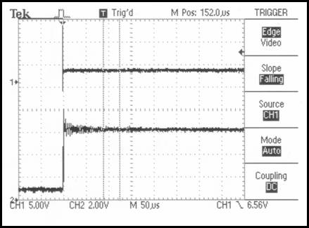
Figure 4
RTP Cell
Immediate response to voltage change
Voltage is at 4600V to compare trace with KD*P crystals
Slight ringing for ~ 180 usec
Amplitude or frequency of ringing does not change with switching frequency.
Ampitude follows changes in cell voltage.
1 meter RG-8 cable from DEI model 4410.
I’m making an initial conclusion that with the higher voltage I am starting to induce a small piezo resonance in the RTP cell. This is a much higher voltage than would ever be required on RTP.
Test 3: Switch cell to KD*P with identical setup used in step 2 and gather data.
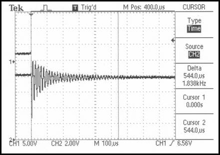
Figure 5
KD*P Cell (Cleveland Crystals model TX2042 20mm)
Voltage is 4600V (λ/2 voltage)
544usec Tsettle to almost perfect state.
Ringing apparent form 1Hz to 400Hz flipping rates.
Voltage change on cell only affects amplitude of ringing.
1 meter RG-8 cable to cell.
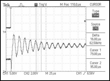
Figure 6
Zoom on trace above. Frequency of oscillation is 62 kHz.
Test 4: Since ringing was observed in step 3, check for equality in (+ to - ) and (- to +) transitions.
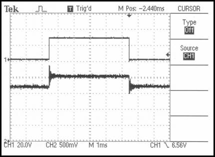
Figure 7
KD*P Cell (Cleveland Crystals model TX2042 20mm)
Voltage is +/- 2300V (λ/4 voltages)
544usec Tsettle.
Ringing identical for (+ to –) or (– to +) transitions.
Ringing apparent from 1Hz to 400Hz.
Voltage change on cell only affects amplitude of ringing.
1 meter RG-8 cable to cell.
Test 5: Switch cable length to a length more appropriate for tunnel installation and gather data. In switching cable length it was immediately apparent that the DEI switch would not be “happy”. The requirement to drive the higher capacitance of the extended cable was too much for the switch and it would trip off in error. I added a 500 ohm power resistor inside the DEI switch to limit the current (and speed) during the transition. The value of this resistance was calculated to keep the transition < 50 usec, but limit the peak current delivered by the switches to the same value as with the DEI recommended cable. (1 meter of RG-8)
Figure 8
Note: The 1 Mohm resistor was not in place during this step. An immediate observation was the length of the ringing is obviously reduced. Slowing down the high voltage transition limited the extent of the ringing.
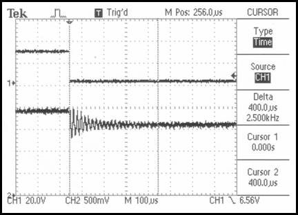
Figure 9
KD*P Cell (Cleveland Crystals model TX2042 20mm)
+/- λ/4 voltages.
Switched to 20 feet of of Reynolds type 167-2669 cable.
Ringing frequency is identical to short cable, so the oscillation observed on the cell is due to a piezo electric resonance of the cell and not due to any problem with the high voltage driver.
Goal is now to squelch the oscillation.
Test 6: Find resistance required to squelch the oscillation.
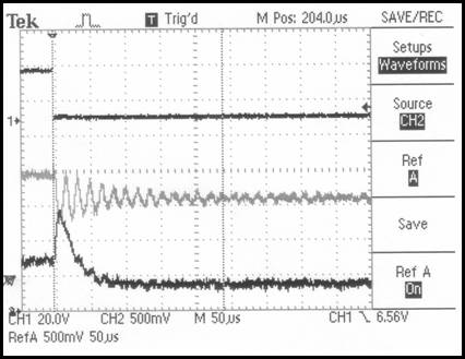
Figure 10
KD*P Cell (Cleveland Crystals model TX2042 20mm)
+/- λ/4 voltages.
20 feet of of Reynolds type 167-2669 cable.
Top trace is HV transition.
Center trace is saved optical transition from previous test
Bottom trace is optical transition with 1M resistor mounted on the cell in series with the HV lead.
Tsettle now 80usec.
Test also performed with:
500k series resistor- Oscillation occurs
2M series resistor- Tsettle doubles
The choice of 1M is proper for this cell and the oscillation is critically damped.
On a side note, If the 1M ohm resistor is built into the end of the drive cable it limits current delivered to <3.2 mA at our λ/2 voltage of 3200V. This is a consideration for Jlab safety to keep the cell in the class 1 (technician safe) electrical safety regime.
Step 7: Verify response of system over a range of flipping frequencies.
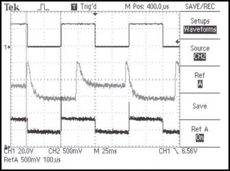
Figure 11
KD*P Cell (Cleveland Crystals model TX2042 20mm)
+/- λ/4 voltages.
20 feet of Reynolds type 167-2669 cable.
Top trace is HV transition.
Center trace is saved optical transition at 1.75kHz flipping frequency (100usec per div)
Bottom trace is optical transition at 10 Hz flipping frequency (25 msec per div).
Conclusions:
- The Qweak experiment requirements can be met. Our present method of gating off 500usec at a 30 hz flip rate results in a DAQ loss of 1.5%. Gating off for 80usec at a 300 Hz flip rate will have a DAQ loss of 2.4%. Not ideal but not bad either. 250 Hz flip rate will have a 2% dead time.
- Perhaps more germane to our present situation, reducing our dead time from 500 usec to 80 usec at our 30 Hz flip rate will improve our DAQ up time by 1.26%.
- Further study is needed to verify that the 20 mm LaserMetrics cell has the same response as the Cleveland Crystals cell used in this experiment. I am hoping to rely on the Happex collaboration to verify this using their DAQ. I will assist as required to ensure our photo-diode response is adequate.