Pockels Cell switching methods. – John Hansknecht
There are 3 basic applications that utilize Pockels Cells.
1. Applications involving Q-switching of lasers with very short (ns) pulses at a given repetition rate. This application usually involves a special cell with 50 ohm impedance. As such, the cell cannot be held in a high voltage state for any significant time. There are numerous manufacturers building fast switches and cells for this application. This type of switch is not discussed in this document.
2. Applications that require a slice of laser light on the order of microseconds. This application is achievable with commercial switches but it has a few caveats that you should be aware of. Most notably is the fact that KD*P cells will “ring” when driven with a fast voltage pulse (rise time < 20us). We have an application that requires a 4us slice of beam with 250ns rise/fall and a flat top with no ringing. The only solution we could find to achieve this was the purchase of an RTP cell. This cell does not ring. The manufacturer specifies this cell to have a minimum 200:1 extinction ratio, but in practice we have achieved extinction of 2500:1 when proper alignment and beam cleanup is performed. This application is not discussed within this document, but the RTP was used to calibrate a KD*P ringing experiment and is discussed here.
3. Applications requiring clean switching between two distinct birefringence states where the cell might remain in a given state for long time periods ( milliseconds to seconds). Our application utilizes a Pockels cell switching between + and - λ/4 birefringence states to create right hand and left hand circular polarization. The remainder of this document will simply refer to this as “helicity state”. This topic is discussed extensively below.
Our reason for being:
Physicists here at the lab have great interest in receiving “parity” quality electron delivery to their physics targets. Our electron beam is produced by photo emission from an electron gun. The laser that drives this photo emission passes through a pockels cell before striking the photo cathode. By controlling the polarization (spin state) of light striking the photocathode, we can control the spin of the electrons produced. “Parity quality” refers to the ability to produce electrons of two distinct spin states where nothing changes except for the spin of the electrons. If the amount of electrons produced differs between the two helicity states, it is seen as an electron current asymmetry. If the trajectory of the electron beam is changed due to Pockels cell steering effects, it is seen as a position asymmetry. We have the daunting task of controlling the polarization asymmetries of light striking the photocathode to low part per million quantities. The selection of the Pockels Cell, the alignment of the cell, and the electronics driving the cell are critical. The final degree of circular polarization from the cell needs to be 99.98% circular (or better) in both helicity states. The remarks in this notebook are dedicated to the electrical drive issues. It should be obvious that any errors in voltage will create errors in final polarization.
When switching a pockels cell for a polarization parity experiment, the following conditions are desirable:
- Symmetry - The transitions between right-hand circular (RHC) and left-hand circular (LHC) must be identical with respect to timing and settling.
- Stability- The voltage must quickly come to a setpoint and remain at that setpoint without overshoot or droop.
- Independent voltage adjustments for each helicity state- A slightly different final voltage is required in each helicity state to compensate for residual birefringence in the cell (or alignment errors).
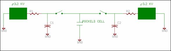
Figure1
Figure 1 represents a diagram of the circuit we have used for all CEBAF experiments to date. (1995-2007). The circuit has provided adequate functionality, but it is not ideal. The two switches are Behlke HTS-81 transistor type switches. They are driven in opposition, so only one can be on at a time. This allows the pockels cell to be at either +3.2kV or -3.2kV (or whatever the supplies are programmed at). The power supplies have been 0 to 4000V programmable (EMCO) high voltage supplies. They are programmed using two DAC channels in EPICS. The supplies are highly regulated and put out a stable voltage, but a rapid surge of current from the supply would cause the voltage regulators to “kick-in” and create an overshoot. This current surge occurs when the pockels cell and associated coaxial cable are switched from one supply to the other to “flip” the polarization state. In an effort to minimize this problem, a large capacitance has been placed on the output of each supply. The R1 and R2 series resistors allow a charge of the capacitors while shielding the supply from the current surge. The capacitors “eat” the transient and the cell settles at the opposite helicity state.
Problems:
- The capacitors droop slightly in voltage after consuming the charge from the cable and cell. There is a long time constant associated with the recharge of these caps. The effect is small, on the order of 10-20 volts out of the 3000V, but in parity experiments this can create unwanted differences. This effect is exaggerated on figure 2 below.
-3KV +3KV
![]()
![]()
![]()
![]()
![]()
![]()
![]()
![]()
![]()
![]()
![]()

Figure
2 (greatly exaggerated example of
the charge time constant that appears across a helicity cycle)
- The drooping was acceptable when all the experiments were running in “toggle” mode. Each helicity state would look just like the next. The droops were equal on the + and – states. When the experiments started to run with a pseudo-random pattern this slow rise time appeared as a problem. Figure 3 shows an example of the differences that now appear when a quartet pattern change occurs in the pseudo-random pattern.
![]()
![]()
![]()
![]()
![]()
![]()
![]()

Figure
3 (Another example with an
exaggerated charge time constant)
A difference in the final voltage reached in any given helicity state appears because the length of time spent in a given state is different. This small change manifests itself as a contribution to the quartet peaks that appear during analysis of the electron beam helicity. To date these affects have been small, but it would be better to eliminate the problem. This requires a redesign of the switch.
- The switch in its present design cannot flip at the 250hz flipping rate desired by the qWeak experiment. This is not due to a limit of the Behlke switches, but is instead a limit of the surrounding circuits and system capacitance and Pockels cell ringing phenomenon. There is presently a 500us dead time on the helicity data acquisition system to account for settling of the cell.
January 2005
Changes in the
design:
We are making some changes to the switch in order to accommodate the qWeak experiment. This experiment is planning on running with a 250 Hz helicity flip rate. The 500us settling time of the present switch would be an unacceptable data loss at this higher flip rate. We would like to reduce the settling time to less than 100us. The attempts to solve the problem involved the purchase of a new commercial high voltage switch from Directed Energy, Inc. . The switch is shown here. The switch is designed for high speed drive and has tightly controlled impedances.
Results of the experiments performed on this new switch can be found here. It should suffice to say that we met and exceeded our goal of 100 us settling time.
One interesting outcome of the testing of this switch was the realization that we have been going about our flipping scheme in the wrong way. In order to speed up the transition, we actually wanted to slow down the high voltage transition so it wouldn’t induce a piezo-electric ringing in the cell. We would be completely satisfied with a controlled rise in voltage to quarter wave voltage in 80 usec, so why are we paying so much money for fast switches that have the capacity to drive a cell in nano-seconds? (a rhetorical question that will be answered later)
Feb 26 2007
The DEI switch was installed in place of the original Behlke design. The switch allowed faster transition times, but also introduced some new problems. It would appear that nothing has changed with regard to asymmetric flipping voltage problems. This new switch has many unknowns inside, so it’s difficult to analyze, but clearly there is still a charged capacitor bank on the plus and minus high voltage rails that can droop in voltage at different rates when flipped with the pseudo-random reversal pattern. Another more troubling problem is the fact that this switch appears to “broadcast” helicity information out to the injector. I hypothesize that this is due to the fast signals being sent to the pulse transformers for gating the MOSFETS. This switch is designed to switch high currents at high speed. As the experiments of 2005 revealed, we don’t actually need the high speed transitions that this switch is capable of providing. We have a 1Meg ohm resistor into the 6 pf Pockels cell capacitance to slow it down. We will continue to look for a better solution.
May 2007
Conceptual Design:
Solve problem with the droop in the voltage rails - Don’t use high voltage switches!
When a switch is used, the cell is immediately connected to the voltage on a power supply “rail”. There will always be a droop in the rail voltage as the system capacitances are recharged. An analog op-amp circuit should be used instead that takes the voltage to a desired value, but NOT all the way to the rail of the power supply. In this scenario, the rails of the power supply are kept slightly higher than the desired op-amp output voltage. Small droops in the rail will not affect the output of the high voltage op-amp. Clearly the circuit shown below in figure 4 could perform the same function as our high voltage switches, but with a final desired differential voltage of +2.56kV and -2.56kV (typical for 780nm on KD*P) the momentary drop in the rails would not be seen on the cell.

Figure 4 An analog solution
The circuit shown can accommodate everything that we require:
- Perfect symmetry
- The PITA programming is still functional.
- The desired rise time of 80us to final settled voltage is possible.
The high voltage amplifier shown can be constructed of using discrete PMOS and NMOS FETs in a symmetrical series high-voltage cascade circuit without difficulty. There are a couple of pitfalls to this design:
- The power requirements on the amplifier bias circuitry.
- The sensitivity to programming voltage. With a gain of about 1000, a small error in programming would result in a rather large error in the final voltage on the cell.
This is a good conceptual design, but will require a significant effort to prototype. – Design on hold for now.
June 2007
Another Conceptual Design:
Goals:
- Circuit should minimize power consumption
- Low cost if possible
- Circuit should have a lower sensitivity to PITA programming changes.
- Circuit should actively measure and respond to the differential voltage appearing across the cell to make voltage error corrections.
The following key concepts will be employed in the design:
- The flipping high voltage will be applied to one side of the pockels cell, just like the Behlke switches do in the traditional design. I will be performing some experiments that will utilize slower switching methods using cheaper discrete FETs in series rather than the using the super-fast (and expensive) Behlke switches. My goal is to settle at the “perfect” voltage within 80us. Going too fast would induce piezo-electric ringing in the cell.
- A voltage divider on the high voltage side of the pockels cell and the low voltage side will be fed to a differential amplifier. The output of this amplifier will be compared with a reference signal and an error signal will be produced. This error is the difference between the measured signal level and the desired signal level
- The error signal will drive an op-amp that applies a voltage to the side of the cell that has traditionally been at ground potential. This op-amp will be capable of correcting up to several hundred volts of error. An Apex Microtechnology PA-97 is envisioned for this circuit. With a 1 MHz bandwidth and power rails up to +/- 450V, it should be fully capable of making rapid corrections to the voltage error.

Figure 5 Conceptual design of new Pockels Cell switch for parity experiments
In operation it would not matter if the high voltage switches on the left had an overshoot or undershoot from the “ideal” final setpoint. The difference amplifier and error amplifiers would actively work to make the differential voltage appearing across the pockels cell perfect as soon as the high voltage is within the range of the op-amp rails. (+/- 450V)
The switch could be designed to be fully capable of operating at the 250hz flip rate and voltage errors will be corrected at a rate of several hundred kHz..
July 2007 (
A web search for high voltage switches yielded something quite interesting. At some point someone discovered that a diode would change its reverse bias leakage based on intensity of light received. (Well, of course… we call that a photodiode) A company called Voltage Multipliers Inc has taken this diode passivation technique and applied it to their high voltage (10kV) diodes.
They have encased the diode in a clear epoxy assembly along with a set of infrared light emitting diodes and they market it as a high voltage opto-coupler. The LED’s can be driven by a grounded or floating circuit, and the light produced causes a change in the reverse bias leakage of the 10kV diode. With proper control of biasing, an optically isolated variable voltage up to 10kV can be realized. Since diodes can be placed in series and the hold-off doubles, higher voltages can be controlled.
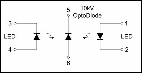
Figure 12
Figure 13
This immediately sparked my interest and I started running the numbers based on the datasheet provided. OC-100-HG datasheet
I was particularly interested in the maximum current achievable with the LED’s at full current.
![]()
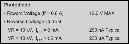
Figure 14
Now 230 uA doesn’t sound like much. After all, the fast commercial high voltage switches I have used thus far have had capacities of many AMPS. But since I only need to change the voltage on a 6pf load in less than 100 us, it might just work out.
230uA is the typical current flowing in the HV diode at 50mA LED drive current, so let’s plug that data into our real world pockels cell drive application. I would be using two of the model OC-100-HG opto-couplers in series. The LED’S for each opto-coupler would be driven in opposition, so the center junction will be pulled to the positive rail (2.56kV) or the negative rail (-2.56kV) depending on the TTL input state.
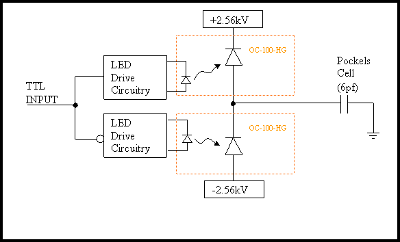
Figure 15
The pockels cell can be viewed as a strictly capacitive device of 6pf. Because these opto-couplers are so small, they can be mounted directly to the top of the cell. This limits the cable capacitance and stray inductances that have plagued us in the past. Without a large capacitance charge transfer, the load seen on the power supply rails will be insignificant. There will no longer be a droop in rail voltage at the moment of the helicity flip.
Running the numbers:
Begin with the cell charged to 2.56KV, so a transition to -2.56KV will be a voltage change of 5120V.
Capacitor charge time =
[Vhigh – Vlow] * C / I = 5120V * 6pf / 230uA = 133
us
This means that in my application of driving a Pockels cell from one high voltage state to the other, the transition time will be 133us if I follow all the guidelines from the OC-100-HG datasheet. One thing is immediately apparent. If I add two more opto-couplers in parallel with the first set I can get twice the current and reduce my transition time to 67us. This value exceeds the best speed I could get out of the cell without inducing a piezo-electric ringing effect (see 2005 studies). Construction of this new switch would require four optocouplers. (At $67 each, this isn’t bad. My previous high voltage switches cost about $8000.)
There are some additional considerations. Just because the datasheet shows a typical current of 230uA doesn’t mean that I can’t pull more current out of the single device. The numbers provided in the datasheet only show the high voltage diode current when normal (nominal) current is applied to the LED’s. The mechanism for LED failure is thermal. It is possible to pulse LED’s for short time periods (<100us) at many times the nominal current. The light intensity produced during this pulse will be much brighter than the nominal output. Since the datasheet doesn’t show the pulsed limits of these photodiodes, we will buy four of these devices and start running some experiments.
September 2007
The OC-100-HG’s arrived and
testing was performed. The transition
measurements matched the predictions perfectly.
If anyone out there is doing these experiments, I should remind you that
it will be close to impossible to perform the measurement of the actual high
voltage appearing on the cell. The currents we are dealing with are quite small
and all oscilloscope leads have impedance.
Any impedance placed at the pockels cell high voltage side will disturb the
actual performance because it disturbs the charge time constants. My measurements were performed using laser
light through the Pockels Cell. The
cells birefringence changes by a known amount for a given voltage applied. By analyzing the light I can determine the
voltage appearing at the junction.
October 2007.
Performance Optimization
The circuit shown in figure 16 below was used to optimize the performance of the OC100HG Pockels cell “switch”. A PIC microcontroller is used to perform timing functions of the four FET transistors. The two LED’s in each OC100HG can be driven in three possible modes:
1. LED’s OFF when FET’s are off.
2. LED’s ON with high current pulse (10 ohm series resistance yields about 1 amp through the LED’s) time limited to 50 micro-seconds.
3. LED’s ON with normal current of about 80 milli-amps (limited by the 120 ohm series resistance).
The D1,D2 LED’s are never on at the same time as the D3,D4 LED’s. They are driven in opposition, just like all of my previous switches. The difference now is that it really wouldn’t be a major problem if they did turn on at the same time. The high voltage diodes will only be passing a couple hundred micro-amps. They are always a relatively high impedance, on or off.
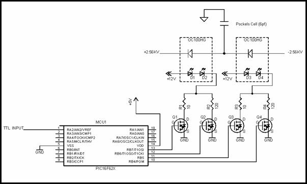
Figure 16
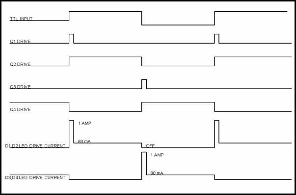
Figure 17
I programmed the microcontroller to provide the drive sequence shown in figure 17 above. The Q1 and Q3 FET’s are only driven for 50us. Thus we are able to drive the LED’s much harder than they would normally operate. The resulting light output is significantly higher and this results in a much faster charge of the Pockels Cell.
The circuit of Figure 16 was prototyped and the system was tested. With 1 amp current sourced, the LED’s of the original OC100HG optocouplers created a transition time of about 40 us. This transition speed corresponds to a current through the optocoupler of 768 micro-amps. This is 3.3 times more current than the datasheet indicates.
There was one unfortunate mistake that I made during the testing. I was testing the circuit at many different repetition rates. Remember that the 50us high current pulse is normally an insignificant power contribution to the LED’s because it is so fast. I started with repetition rates of 10 Hz, then moved to 100 Hz and eventually 1kHz. Unfortunately, I didn’t stop at 1kHz. At these high speeds, 50us starts to become a significant percentage of the “on” time. Result: LED’s burned out and the system stopped working.
Once I figured out the problem, I added code to the microcontroller that limits the maximum flip rate to 1.2 kHz, so the flip rate will follow the TTL drive signal in repetition rate until it reaches 1.2 kHz. At this time it will lose phase lock and clip at the max rate.
The failure of the LED’s may have been a blessing in disguise. I now had two failed OC100HG’s at my disposal. I decided to use a saw to remove the LED’s, polish the area where the LED’s were cut away, and then provide a mounting fixture to test my own LED’s. I was hoping to find an LED that provides higher power and thereby faster time response at lower drive currents.
As I cut away the LED’s, I realized that the original design of the OC100HG may have an Achilles heel. The LED’s that were used were standard 850nm T-13/4 (5mm) in a clear package. This clear package has focusing properties that direct the LED die output light forward into a cone with about 10-20 degrees of divergence. It is my belief that when this clear package is molded into the clear epoxy of the OC100HG, the epoxy served as an index matching medium for the LED lens, thereby destroying all focusing properties of the original LED. Without focusing, the radiant energy striking the high voltage diode is greatly diminished. A change in the design may yield higher current transfer ratios.
Modifying the OC100HG for higher current transfer:
I purchased new OSRAM high power infrared LEDs with a 3 degree emission divergence. Model SFH 4550. The LED is rated at a typical 700 mW/sr when powered at 100mA.
DANGER:
THIS LED PRODUCES INVISIBLE LIGHT AT POWER LEVELS EQUIVALENT TO A CLASS
4 LASER. DO NOT MAKE AN ATTEMPT TO LOOK
INTO THIS LED WITH THE NAKED EYE OR WITH COLLECTING OPTICS AS SERIOUS RETINAL
DAMAGE MAY OCCUR!
Researchers wishing to analyze the
output of this diode should use the standard tools and precautions used during
laser research. There are some key
differences. The nominal hazard zone for
this device is relatively short because of its divergence, so diffuse or
specular reflections should not be a problem.
I can recommend three tools:

Infrared viewer card. Infrared viewer scope A
standard USB camera
As you can see, the first two
items are designed specifically for laser research, but the third option is
also quite useful. Most cheap CCD
cameras are sensitive to the 850nm light produced by this LED and they can be
as cheap as $15.
As you can see by my warning, even run in CW mode, this is a very high power LED, but the datasheet also provides data showing the power intensity when pulsed at higher currents.
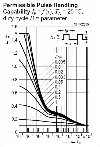
Figure 18 Peak pulse current permitted vs time of pulse and duty cycle.
When pulsed at 1 Amp for less than 100us, this LED emits 7 Watts/sr at its forward solid angle! At low rep rates, we are even permitted to pulse this LED at 1.5 Amps.
The images in figures 19-23 show the modifications that I made to the OC100HG to create my new switch design. I now have three LED’s focused on each of the OC100HG high voltage diodes. Since the LED is mounted external to the polished diode mount, the focusing properties are not disturbed during the air to plastic transition.
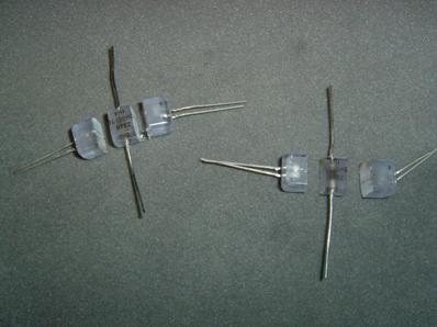
Figure 19. LED’s cut away from OC100HG’s and discarded

Figure 20. Remaining HV diodes in polished housing
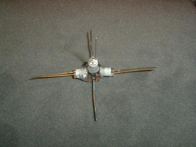
Figure 21. New LED mounting tubes placed around diode
- 3kV + 3kV To Cell
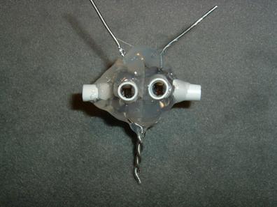
Figure 22. Both HV diodes joined in series. Mounting tubes for 6 LED’s. Opaque barrier between individual units.
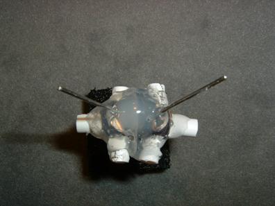
Figure 23. Top view of switch.
Switch performance:
I started testing the switch with modest currents through the new LED’s. I placed a 15 ohm series resistance at R1 and R3 (see figure 16). This provides a 50us pulse of approximately 450mA through the new LED’s. I also placed 180 ohms on R2 and R4 to provide a hold current of 42mA through the LED’s, which is quite modest indeed.
The proof is in the pudding
so they say.
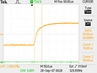
Figure 24. Pockels cell transition of 5160V as analyzed by light passing through
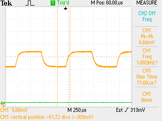
Figure 25. Pockels cell flipping at 1kHz to +/- λ/4 birefringence states. (780nm)
I briefly experimented with higher peak currents on the 50 us pulses by reducing the values of R1 and R3, but the Pockels cell would begin to ring due to piezo electric effects. There was no need for me to go any further with this particular experiment, so I boxed up my prototype and installed it in the injector tunnel.
Link to DATA taken during tunnel installation
The system in the injector tunnel is now completely floating with respect to earth ground. We will take parity measurements and determine if this is fine. If we wish, it is easy to ground the system at a single point. The TTL drive input comes from a fiber optic receiver. The small power necessary to run the PIC microcontroller and LED drive circuitry comes from a wall wart type power supply that does not carry an earth ground. The DC-DC high voltage power supplies are also floating and fed from a wall wart supply with no ground.
(schematic to be posted soon)
Some final remarks about the OC100HG
It is obvious to me that this modified OC100HG is capable of much higher pulsed currents than I presently need for this application. I will probably perform the tests on a future date to test the limits of the device. I have an RTP (Rubidium Titanyl Phosphate) Pockels cell that will not ring at higher transition speeds, so the OC100HG may be useful for driving it for faster laser beam chopping applications. This device could be useful for biasing electrostatic plates in an accelerator beamline for kicking the beam.
It is also obvious that the OC100HG can be used for numerous analog applications. An analog drive on the LED’s will yield an analog current swing. It would be fairly easy to create a high speed attenuator that can be used to stabilize intensity fluctuations from a noisy laser. One simply needs to add a linear polarizer after the Pockels cell and close a servo loop with a downstream power measurement. If a pulsed chopper drive scheme is used on the LED’s, the device could achieve large voltage swings at high speed. Present commercially available “noise eaters” are limited in bandwidth at higher extinction ratios. I think this device could be used to solve this problem.

This work was supported by the U.S. DOE under Contract No. DEAC05-84ER401050.