|
|
-
Optimum performance for (A) low-, (B) medium-, and (C) high-capacitance
charged-particle or heavy-ion detectors
-
Extremely low noise
-
Accepts 0 to ±1 kV bias
|
-
Separate fast-timing output signal with rise time from <5
ns
-
Operates in vacuum
-
Small size
|
| The ORTEC Models 142A, 142B, and 142C Preamplifiers
are low-noise, fast-rise-time, charge-sensitive preamplifiers designed
for optimum performance with charged-particle or heavy-ion detectors. |
| The Model 142A is optimized for extremely
low noise and fast timing for detectors with capacitance up to 100 pF.
This makes it the ideal selection for high-resolution alpha- and beta-particle
spectroscopy applications. |
| Model 142B is optimized for extremely low
noise and fast timing for detectors with capacitance greater than 100 pF
but less than 400 pF. |
| Model 142C is optimized for extremely low
noise and fast timing for detectors with capacitance greater than 400 pF. |
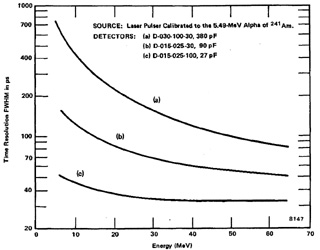
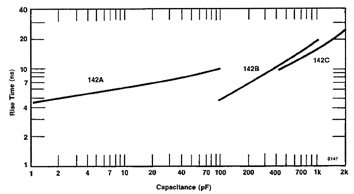
| These preamplifiers have a separate fast-timing
output with pulse widths of ~ 50 ns and rise times ranging from less than
5 ns for 0 pF detectors to less than 20 ns for 1000 pF detectors. This
timing output, when used in conjunction with ORTEC's standard electronics,
provides excellent time resolution (Fig. 1); also,
its fast-differentiated shape often permits direct coupling to the timing
discriminator. |
| The performance of many spectroscopy systems
can be enhanced by these preamplifiers being able to operate in vacuum
enclosures. This allows the input cable length to be minimized. The small
size of the preamplifier is of significant importance when operating in
such enclosures due to the limited space available. |
|
PERFORMANCE
|
| Performance specifications apply to E output unless stated
otherwise. |
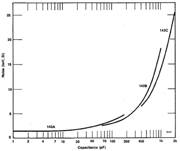
NOISE (see Fig. 2)
| Model |
Detector
Capacitance
(pF) |
Maximum
Noise
(keV)(Si) |
| 142A |
0 |
1.60 |
| 142A |
100 |
3.40 |
| 142B |
100 |
3.20 |
| 142B |
1000 |
19.00 |
| 142C |
400 |
7.20 |
| 142C |
1000 |
14.50 |
| 142C |
2000 |
27.00 |
|
| INTEGRAL NONLINEARITY £0.03%,
0 to ±7 V open circuit or ±3.5 V terminated in 93
W. |
TEMPERATURE INSTABILITY
142A <±50 ppm/°C from 0 to 50°C.
142B <±100 ppm/°C from 0 to 50°C.
142C <±100 ppm/°C from 0 to 50°C. |
OPEN LOOP GAIN
142A >40,000.
142B >80,000.
142C >80,000. |
CHARGE SENSITIVITY (Si equivalent)
142A Nominally 45 mV/MeV.
142B Nominally 20 mV/MeV.
142C Nominally 20 mV/MeV. |
ENERGY RANGE
142A 0 - 200 MeV.
142B 0 - 400 MeV.
142C 0 - 400 MeV. |
E2CRP Maximum energy-squared count-rate
product:
142A 1.5 x 10⁷ MeV2/s.
142B 3 x 10⁷ MeV2/s.
142C 3 x 10⁷ MeV2/s. |
RISE TIME (0 to 0.5 V pulse at E output on 93-W load)
142A <5 ns at 0 pF; <12 ns at 100 pF.
142B <5 ns at 100 pF; <25 ns at 1000 pF.
142C <11 ns at 400 pF; <20 ns at 1000 pF. |
DECAY TIME
142A Nominally 500 µs.
142B Nominally 1000 µs.
142C Nominally 1000 µs. |
RECOMMENDED RANGE OF INPUT CAPACITANCE
142A 0 to 100 pF.
142B 100 to 400 pF.
142C 400 to 2000 pF. |
| DETECTOR BIAS VOLTAGE ±1000 V maximum. |
|
|
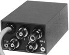
INPUTS
|
| INPUTS Accepts positive or negative charge input
(normally from a semiconductor detector) from any type detector; BNC connector. |
| BIAS Accepts detector bias from supply and applies
it to detector through the INPUT connector; maximum ±1000 V; SHV
connector of ORTEC type C-38. |
| TEST Input for pulse generator to test and calibrate
the system; BNC connector. |
| POWER Input power through 10-ft captive power cable
from ORTEC main amplifier or ORTEC Model 4002P Portable Power Supply. |
|
OUTPUTS
|
| E Positive or negative linear tail pulse for energy
measurement. BNC connector. |
| T Negative or positive linear fast-clipped pulse
for timing. This output is generated using an inverting transformer that
differentiates the energy output. Its rise time ranges from <5 ns to
<25 ns. BNC connector. |
|
ELECTRICAL AND MECHANICAL
|
POWER REQUIRED
142A +24 V, 20 mA; -24 V, 10 mA; +12 V, 15 mA; -12 V, 15 mA.
142B +24 V, 40 mA; -24 V, 10 mA; +12 V, 15 mA; -12 V, 15 mA.
142C +24 V, 40 mA; -24 V, 10 mA; +12 V, 15 mA; -12 V; 15 mA. |
WEIGHT
Net 0.32 kg (0.75 oz)
Shipping 1.25 kg (2.75 lb) |
| DIMENSIONS 3.81 x 6.10 x 13.3 cm (1.5 x 2.4 x 5.25
in.). |
|
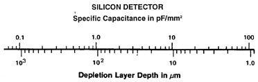
SELECTION GUIDE TO 142A, 142B, or 142C
|
| To choose among Models 142A, 142B, or 142C: |
| 1. Find the depletion depth of your detector. If
it is an ORTEC detector, the last group of 2 to 4 digits is the depth in
µm. |
| 2. Find the depletion depth on the graph in Fig.
4 and read the capacitance in pF/mm2 on the top part of
the chart. |
| 3. Multiply the area of your detector in mm2.
This is the middle three-digit number for an ORTEC detector. Choose a Model
142A if the capacitance is less than 100 pF, a Model 142B is the capacitance
is more than 100 pF but less than 400 pF, a Model 142C if the capacitance
is greater than 400 pF. An ORTEC D-025-100-200 detector will have about
1 pF/mm2 for its 100-µm depletion depth. This, then, is
200 pF for the 200 mm2 area, and a Model 142B Preamplifier is
preferred. |
|
ORDERING INFORMATION
|
| To order, specify: |
| Model |
Description |
| 142A |
Preamplifier (for 0 to 100 pF) |
| 142B |
Preamplifier (for 100 to 400 pF) |
| 142C |
Preamplifier (for 400 to 2000 pF) |
|
|