SVT Detector Description
Quick Overview
For the 12 GeV upgrade, the CLAS12 experiment has designed a Silicon Vertex Tracker (SVT) using single sided microstrip sensors fabricated by Hamamatsu. The sensors have graded angle design to minimize dead areas and a readout pitch of 156 μm, with intermediate strip. Double sided SVT module hosts three daisy-chained sensors on each side with full strip length of 33 cm. There are 512 channels per module read out by four Fermilab Silicon Strip Readout (FSSR2) chips featuring data driven architecture, mounted on a rigid-flex hybrid. Modules are assembled on the barrel using unique cantilevered geometry to minimize amount of material in the tracking volume.
SVT Physics requirements
Essential parts of the physics program, such as GPDs, require tracking of low momentum particles with few percent momentum and about one degree angle resolution at large angles.. This is achieved by the SVT. Silicon detector technology makes an excellent match to the central tracking system in the CLAS12 configuration, small space and high luminosity operation that is needed for accurate measurements of exclusive processes at high momentum transfer. SVT provides standalone tracking capabilities in the central detector region:
- Measure recoil baryons and large angle pions, kaons
- Polar angle θ coverage:

- Azimuthal angle φ coverage: over 90% of

- Momentum resolution:
- Angle resolution:
 10
10  20 mrad,
  mrad
mrad - Tracking efficiency:

- Match up tracks with hits in the CTOF for
 vs. p measurement (particle ID)
 - Stable operation in 5 Tesla magnetic field at instantaneous luminosities

Expected integrated luminosity per year 500  . Radiation dose for forward sensors (carbon target) is 2.5 Mrads.
Detector design and simulation
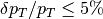
The current design of the Barrel Silicon Tracker (BST) comprises 21504 channels of silicon strip sensors in six layers (three concentric polygonal regions that have 10, 14, and 18 double sided modules mounted back to back). There are three daisy-chained sensors per layer (six per module). Each layer has 256 strips with linearly varying angles of  . The readout strips have a constant
  pitch of
  .
.
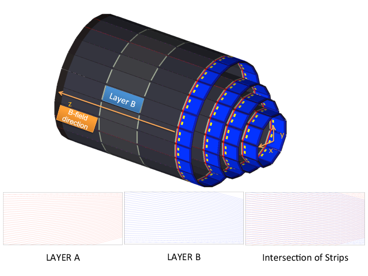
Fig. 1 Side view of the SVT detector.
According to the results of JEANT simulation of the SVT, a resolution of 50 μm in the bending plane is needed to measure, with a precision better than 5%, tracks with momentum up to 1 GeV. Silicon Vertex Tracker uses single sided 320 μm thick microstrip sensors fabricated by Hamamatsu. The sensors have graded angle design to minimize dead zones and a readout pitch of 156 μm, with intermediate strip.

Fig. 2 Results of Monte Carlo Simulation for the SVT momentum resolution.
SVT Module
To minimize multiple scattering a unique module design with extra long 33 cm strips has been developed to reduce material budget to 1% of radiation length per region (two silicon planes) for normal incidence tracks, which is essential for low momentum tracking. The SVT modules are cantilevered off a water-chilled cold plate, designed to remove the heat generated by the electronics, located only at one end of the module. Readout electronics is outside of the tracking volume.
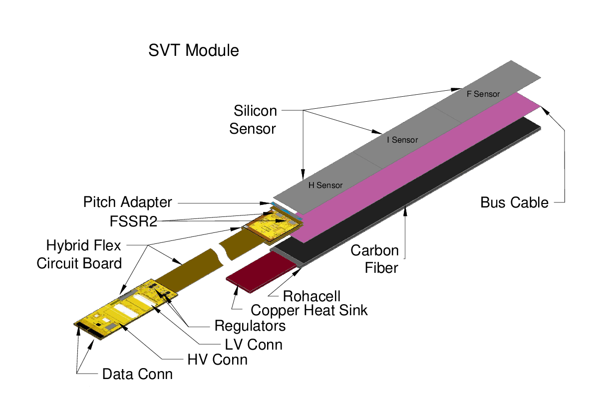
Fig. 3 Layout of the SVT module.
Double sided SVT module hosts three single sided daisy-chained microstrip sensors fabricated by Hamamatsu on each side. All modules have 3 types of sensors: Hybrid, Intermediate, and Far. Sensors are cut from 6 inch wafers, 2 sensors per wafer. All sensors have the same size, 112  42 mm. All SVT modules are identical.

Fig. 4 SVT module in the carrier box.
Sensors are mounted on a composite backing structure composed of Rohacell 71 core, bus cable, and carbon fiber. The carbon fiber skin is made from K13C2U fibers oriented in a quasi-isotropic (45/-45/0) pattern. It is co-cured with the bus cable, which is made from a Kapton sheet with 3 μm thick copper traces, which are 0.5 mm wide; traces on one side provide high voltage to the sensors, on the other side they form a 6 6 mm copper mesh over the entire area for grounding the carbon fiber. The Rohacell core under the hybrid board is replaced by a copper heat sink to remove  2 W of heat generated by the ASICs. At the downstream end of the module, the Rohacell core is replaced by a polyether ether ketone (PEEK) core.
Pitch adapter serves to match the 156 μm sensor readout pitch to the 50 μm FSSR2 bonding pad pitch. The pitch adapter is a glass plate with metal traces made of an alloy of aluminum and copper. The alloy improves electromigration hardness and bonding. The metal layer is sputter deposited. The passivation layer protects the aluminum traces from damage and is made from  . There are 512 channels per module read out by FSSR2 chips, mounted on a hybrid.
A readout system which instruments both sides of a module with a single rigid-flex Hybrid Flex Circuit Board (HFCB), has been developed by JLAB and fabricated by Compunetics Inc. The HFCB is located on the upstream end of the module. It hosts four FSSR2 ASICs, two on the top and two on the bottom side. The hybrid areas are connected by a 10 mm-long wing cable. Data is transferred from the hybrid via the flex cable to the level one connect (L1C) board. The L1C has two high density Nanonics connectors for data and control lines, Molex Micro-Fit 9-pin connector for high voltage ( 85 V) bias to the sensors, and AMP Mini CT 17 pin connector for low voltage (2.5 V) power to the ASICs. There are 12 layers in rigid part and 6 layers in flex part. Control, data, and clock signals do not cross the ground plane splits. Clock signals are located on a separate layer. Guard traces are routed between output, clock, and power lines. Separate planes are provided for analog and digital power. To reduce noise on these planes, regulators and bypass capacitors are added. High voltage filter circuits and the bridging of high and low voltage return lines are located close to the ASICs. Decoupling capacitors for power transmission are placed at transitions between flex and rigid materials.

Fig. 5 Hybrid Flex Circuit Board (HFCB).
Readout system
The FSSR2 ASIC has been developed at Fermilab for the BTeV experiment cite{FSSR}. It was fabricated by Taiwan Semiconductor Manufacturing Company in the 0.25- μm CMOS process. The chip features a data-driven architecture (self-triggered, time-stamped). Each of the 128 input channels of the FSSR2 ASIC has a preamplifier, a shaper that can adjust the shaping time (50 125 ns), a baseline restorer (BLR), and a 3-bit ADC. The period of the clock called beam crossing oscillator (BCO) sets the data acquisition time. If a hit is detected in one of the channels, the core logic transmits pulse amplitude, channel number, and time stamp information to the data output interface. The data output interface accepts data transmitted by the core, serializes it, and transmits it to the data acquisition system. To send the 24-bit readout words one, two, four, or six Low Voltage Differential Signal (LVDS) serial data lines can be used. Both edges of the 70 MHz readout clock are used to clock data, resulting in a maximum output data rate of 840 Mb/s. The readout clock is independent of the acquisition clock. Power consumption is le 4 mW per channel. The FSSR2 is radiation hard up to 5 Mrad.
Each of the four FSSR2 ASICs reads out 128 channels of analog signals, digitizes and transmits them to a VXS-Segment-Collector-Module (VSCM) card developed at Jefferson Lab. The event builder of the VSCM uses the BCO clock timestamp from the data word of each FSSR2 ASIC and matches it to the timestamp of the global system clock, given by the CLAS trigger. The event builder buffers data received from all FSSR2 ASICs for a programmable latency time up to 16 μs. The VSCM is set up to extract event data within a programmable lookback window of 16 μs relative to the received trigger. The trigger latency is expected to be 8 μs.
Calibration of the readout chain
Since the SVT modules are designed with a binary readout system, the analog channel response cannot be measured directly. Instead, the analog response is reconstructed by injecting a calibration charge on the channel and measuring the corresponding occupancy over a range of threshold values. Noise is measured using external, low frequency calibration charge injected in the absence of signal. The injected charge is shaped and amplified in the analog circuitry to form an output signal. The discriminator threshold determines whether or not the output signal corresponded to a hit. The probability that the injected charge produces a hit depends on the setting of the discriminator threshold. The average hit probability is measured by repeating the process of injecting charges and counting the fraction of readout triggers that produced a hit. This measurement is repeated over a range of threshold settings to produce an occupancy plot. The occupancy plots were measured setting the pulser amplitude at fixed values and changing the comparator thresholds. Each point of an occupancy plot represents the percentage of times that the comparator fires for a certain value of injected charge. In between the high and low threshold regions, the occupancy curve is described by an error function, or S-curve, which can be fitted to the occupancy histogram for each channel, producing a mean value (discriminator threshold) and standard deviation (noise). The conversion from mV to electrons is performed considering a nominal value for the FSSR2 injection capacitance of 40 fF.
Fig. 6 Typical threshold dispersion within a chip.
Threshold dispersion is defined to be a standard deviation of the distribution of means obtained from the parameters of the complementary error function fit. The noise and threshold dispersion constants for each individual detector channel are measured and the values are used by the zero-suppression algorithms implemented in the core logic of the FSSR2 and by calibration procedures to identify defective channels. A comparison of the noise for 33 cm strips with the threshold spread demonstrates that the threshold spread is negligible compared to noise and will not affect efficiency and noise occupancy.
Results of the Full Chain Test
No significant correlated noise has been observed between the channels of the same chip, between the chips of the same module or between the closely placed modules. Measured average channel noise is comparable with estimated contributions of different noise sources.

Fig. 7 Typical input noise on a single chip of an SVT module.
Longer silicon strips have higher capacitance and thus a higher expected value for the input noise. Noise calibration accounts for the different strip lengths and pitch adapter layouts that affect the input capacitance of the preamplifier.

Fig. 8 Noise occupancy histogram with no charge injection is shown below. It probes the tail of the noise distribution, which can show effects masked by the higher occupancy at low thresholds. Channel noise allows setting a 3  threshold at 20 keV level.

Fig. 9 Channel noise occupancy vs. DAC hit/no-hit threshold (in DAC bins, one DAC bin corresponds to 3.5 mV).
Calibration Software
SVT calibration scan takes about 20 minutes and is done with a terminal command:
clasrun@svtsystem1> calibration
During this scan the calibration of the SVT modules connected to the upper VSCM channels is performed first, then the modules connected to the lower channels are calibrated. The scan will produce the ASCII calibration files, one file for each chip. The directory in which these files are created is automatically created and is named by the time stamp when the scan started. The calibration suite is launched with a command:
clasrun@svtsystem1> java –jar svtcalibration.jar
The calibration GUI will be opened and the directory containing the calibration files can be selected for processing from the menu. The processing of the calibration files takes 5-10 min depending on the CPU. When the analysis is done, the results of the SVT calibration will be presented in summary plots by pressing the “SVT” button. The calibration GUI (Fig. 10) has several windows. On the left side the detector view is shown. It displays the layout of the SVT modules in the barrel. Each module is represented by 4 rectangles according to the number of readout chips. Initial rectangle color is blue. The rectangles are placed in layers, the inner layer corresponds to the bottom sensors, the outer layer – to the top sensors. Region and layer numbering starts from 1 (inside out). The chips are numbered as 1 (U1 and U3), and 2 (U2 and U4). The module (sector) numbering starts from the bottom of each region.
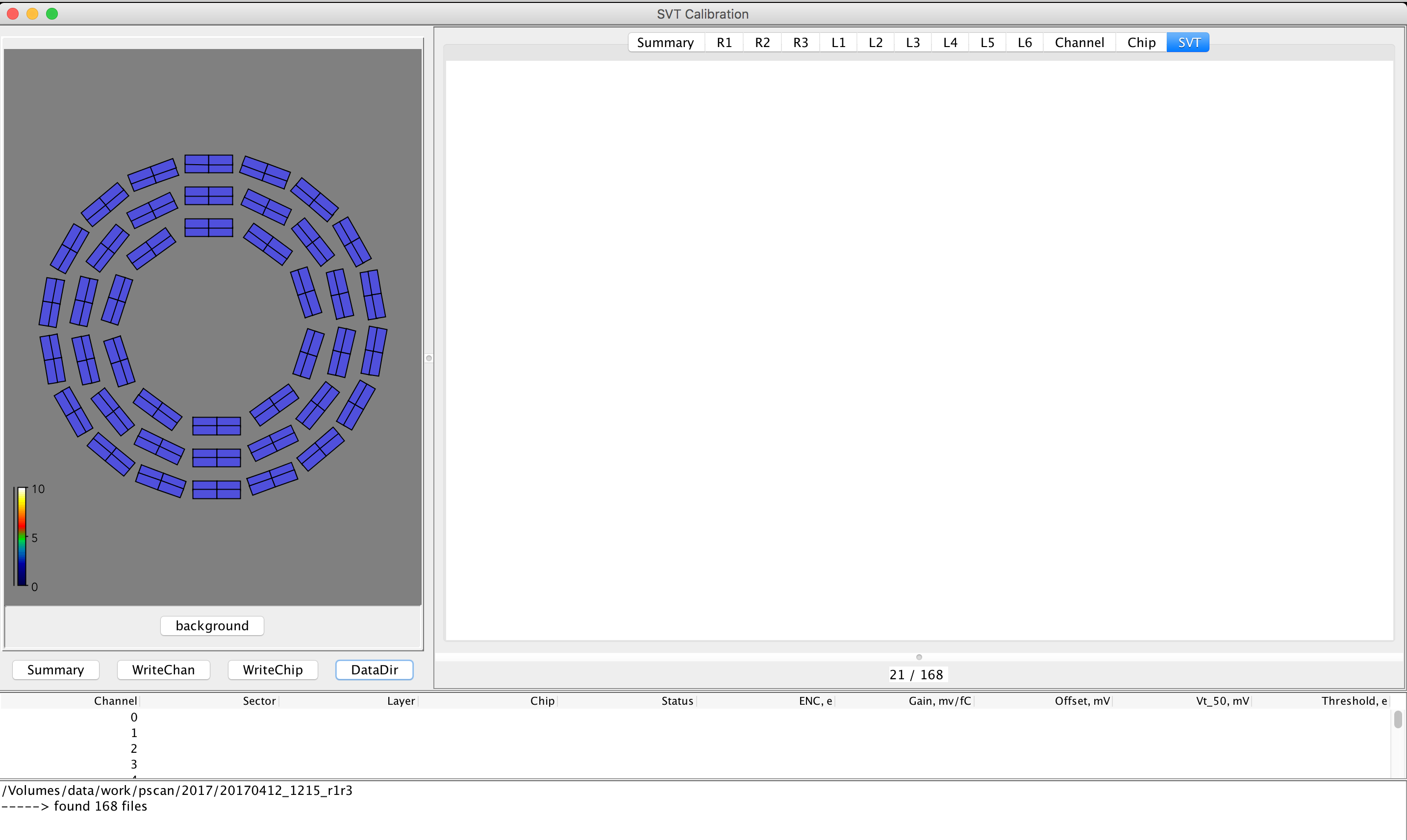
Fig. 10 SVT Calibration GUI
On the top of the detector view there is a status panel which is filled with information when a specific chip is selected. On the bottom of the detector view there are buttons to display the summary of the calibration analysis, to write the calibration tables as ASCII files for each chip or channel, and to select the calibration data directory and start processing the calibration scan. On the right side of the detector view there are tabbed embedded canvases. The tabs represent different parts of detector. Region tabs (R1 to R3) display calibration plots for each region, layer tabs (L1 to L6) display plots for each layer. SVT tab displays calibration plots for the whole detector. Chip and Channel tabs show plots on a chip and channel (strip) level. Summary tab shows a histogram of operational percentage for the SVT and it’s regions. On the bottom of the canvas window there is an information panel showing the progress of the analysis (the number of processed chips and the total number of the chips in the calibration scan). Below the button panel there is a table which displays the calibration constants for each channel of the selected chip. On the bottom of the calibration GUI there is a log panel. To start processing the calibration scan the directory containing the calibration data should be selected by pressing the “DataDir” button. The analysis will start when directory is chosen. The selected directory and the number of files in it (one file per each chip) will be displayed in the log view. The progress can be checked on the information panel. When analysis is done the log view will display the summary of the calibration data analysis. This summary can be also displayed by clicking on the “Summary” button as shown in Fig. 11.

Fig. 11 Calibration summary window
The summary starts with a list of bad channels found, their location (layer, region, sector, chip, channel number, ENC, channel status (N – noisy, D – dead, O – open), followed by the operational percentage, information about the bad channels, mean chip gain and ENC for each region and for the whole detector. Chips with bad channels are marked with maroon color in the detector view. If there are no bad channels found, the chip rectangle color is teal.

Fig. 12 SVT Noise and Gain Calibration Summary Canvas
“SVT” tab has plots of ENC and gain for each chip and channel (Fig. 12). Channel histograms are fit with a Gaussian. Mean chip gain and noise distributions are calculated for all the channels of U1/U3 chips, and for the first 50 channels of U2/U4 (33 cm long strips). Channel ENC plot has a main peak corresponding to the full-length strips with mean around 1600 e, and a shoulder on the left side corresponding to the channels with shorter strips. The gain distributions are centered on ~85 mV/fC. The “Summary” tab has a histogram (Fig. 13) displaying operational percentage of the SVT (first bin), and of the regions (bins 1, 2, and 3).

Fig. 13 Detector operational percentage histogram
Region and layer tabs have the same plots as the “SVT” tab, filled for each region and layer separately (Fig. 14, Fig. 15).

Fig. 14 Calibration plots for Region 1
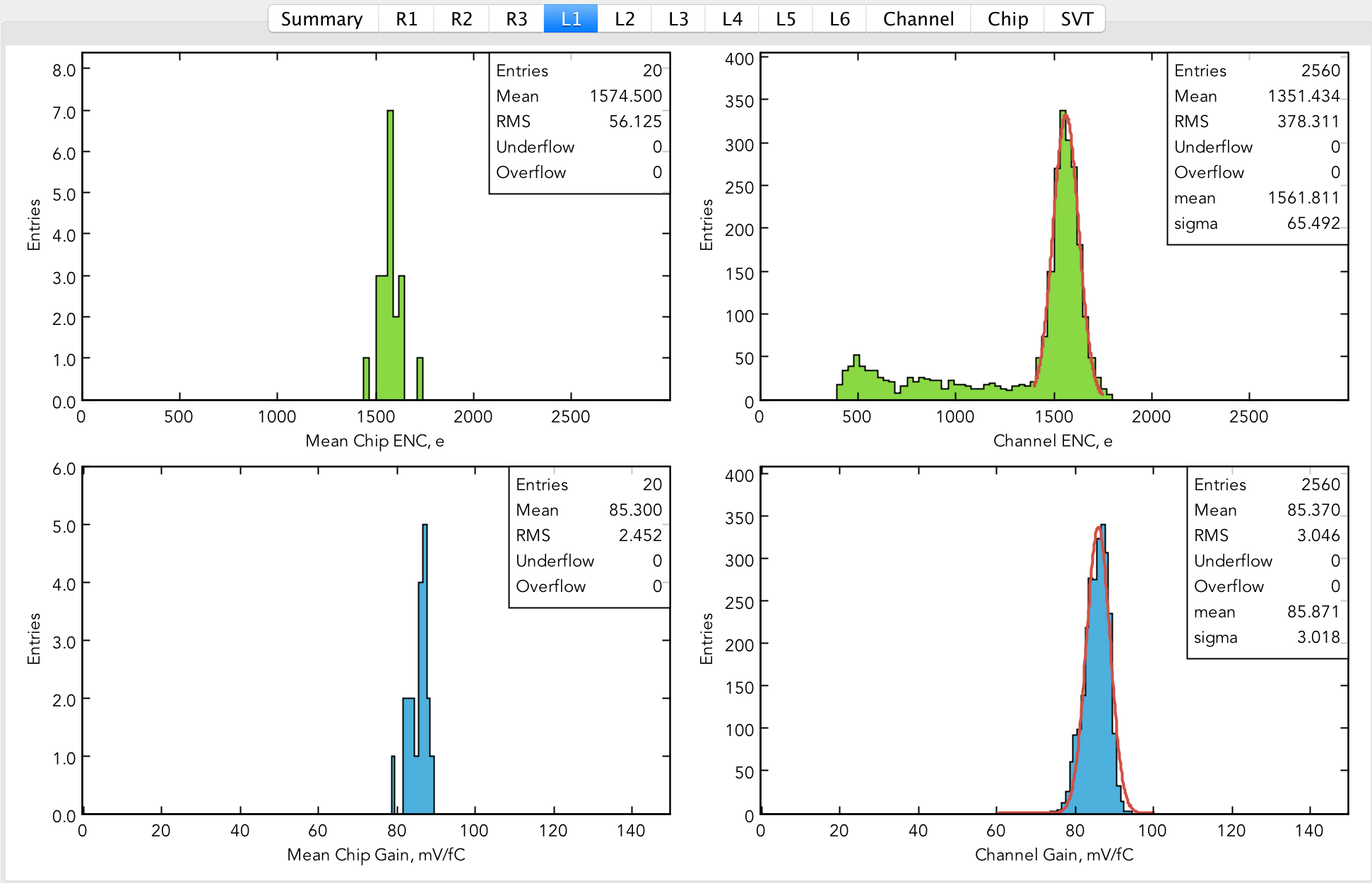
Fig. 15 Calibration plots for Layer 1
Chip level plots can be displayed by selecting a chip in the detector view on the left side. The selected chip is marked with red color. The status panel on the top of the detector view is filled with information about the selected chip (layer, region, sector), crate, slot, VSCM channel (with blue color), mean ENC and gain of the chip. There are 6 pads in the “Chip” canvas: ENC vs. channel plot, gain vs. channel plot, gain dispersion histogram, threshold dispersion histogram, offset vs. channel plot, and Vt50 vs. channel plot (Fig. 16). For U1/U3 ENC and gain are uniformly distributed along the channels with slight shoulders at the chip edges. Mean ENC is about 1600 e, gain about 85 mV/fC. Offset and Vt50 are also uniformly distributed along the channels, with Vt50 around 300 mV and offset within tens of mV.

Fig. 16 Typical calibration plots for U1 or U3 readout chips
The color of the chip rectangles which have been previously selected, will change to grey, if the chip has no bad channels, or to yellow, if there are bad channels found. ENC vs. channel plot for U2/U4 has a slope starting at the channel 50 when the length of the strips starts to drop (Fig. 17). Mean ENC and gain for these chips are calculated for the first 50 channels.
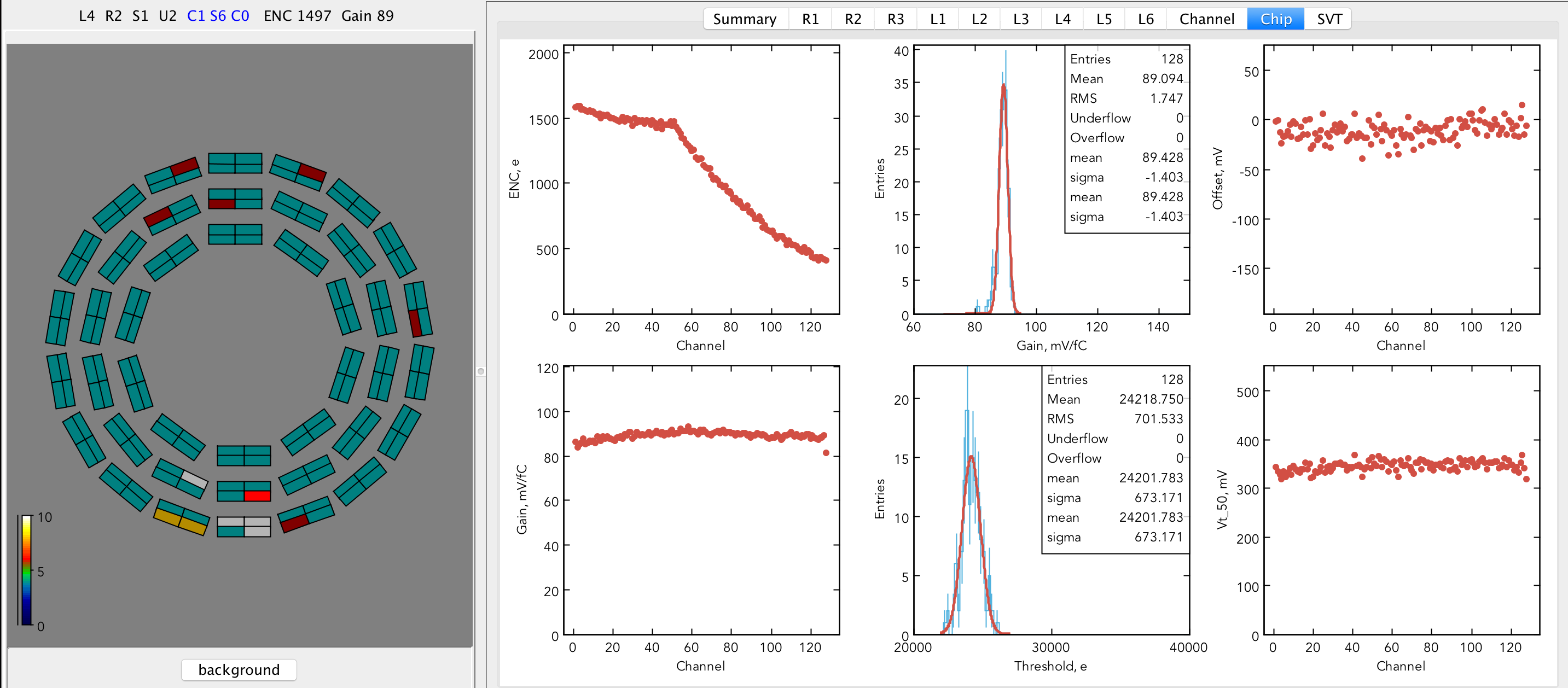
Fig. 17 Typical calibration plots for U2 or U4 readout chips
In case where a bad channels were identified, the status panel would have their status (O – open, D – dead, N – noisy) and numbers in red color. An open channel would have low noise compared to adjacent channels (Fig. 18). Dead channel would have ENC = 0.

Fig. 18 Example of a chip with an open channel
At the bottom of the histogram canvas there is a channel summary table (Fig. 19). Each line corresponds to a single SVT readout channel (strip). The columns contain numbers for the channel location, status, ENC, gain, offset, Vt50, and threshold. Channel status is filled with an empty string for good channels, and with “open”, “dead”, “noisy” strings for bad channels.
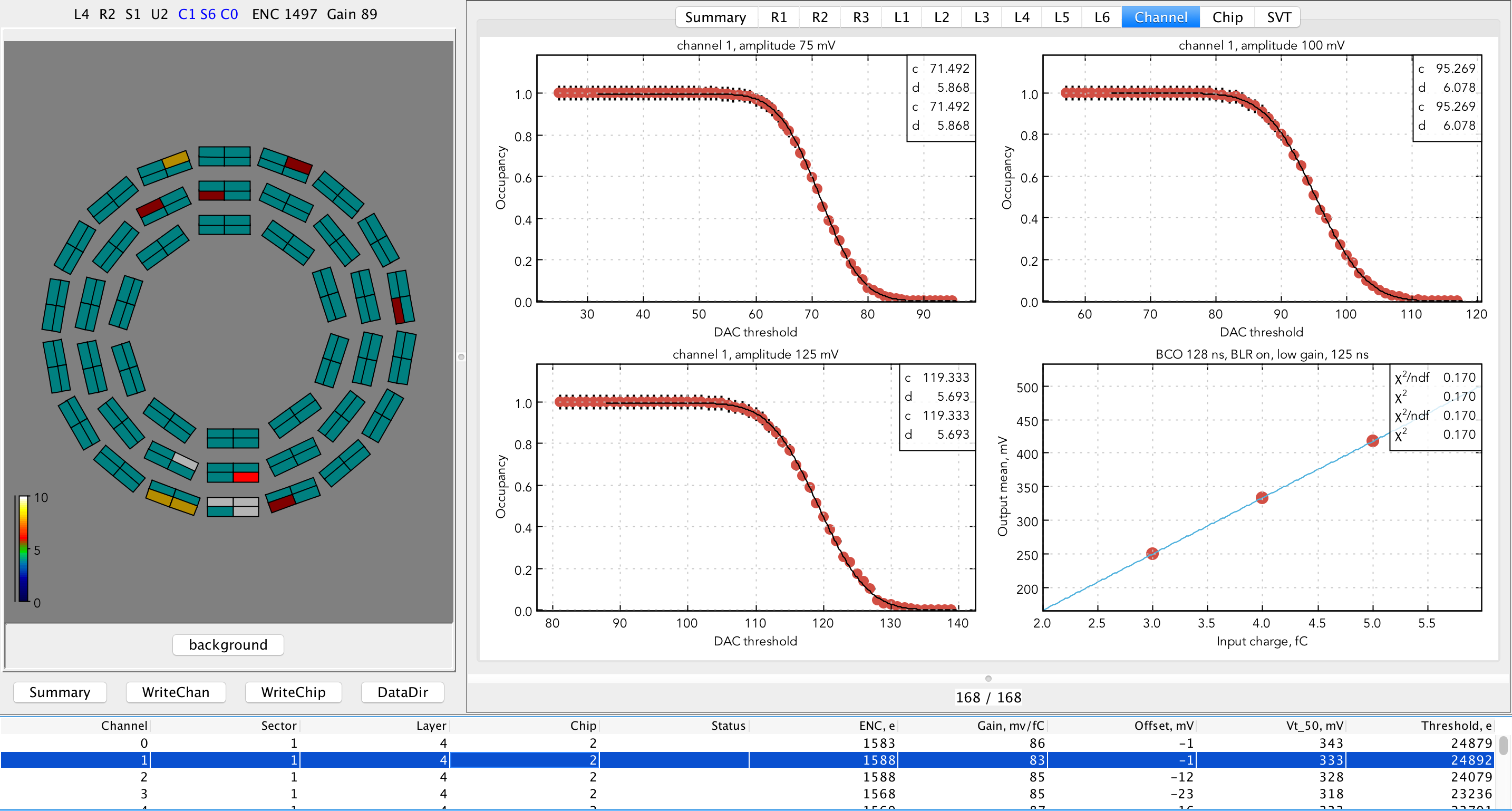
Fig. 19 Typical calibration plots for a single readout channel
The channel occupancy and response curve plots can be shown on the “Channel” canvas by selecting the line in the table. The occupancy scans are done with calibration amplitudes of 3, 4, and 5 fC. Calibration constants for a channel are saved for the amplitude of 3 fC. The occupancy scans are fit with an error function. The parameter d corresponds to the Gaussian sigma of channel noise (in DAC counts). The parameter c corresponds to the amplitude of injected calibration charge. The response curve is fit with a line. The slope of this line corresponds to the channel gain in mV/fC, the intersect with Y axis provides the offset in mV. In the rare cases where occupancy scan fit fails (Fig. 20) the initial parameters of the erf should be adjusted by the SVT expert. In this example the channel was misidentified as noisy (see the status column) because even though 2 out of 3 erf fits converged, the fit for a scan with calibration charge equal to 3 fC which is used for ENC analysis, failed.
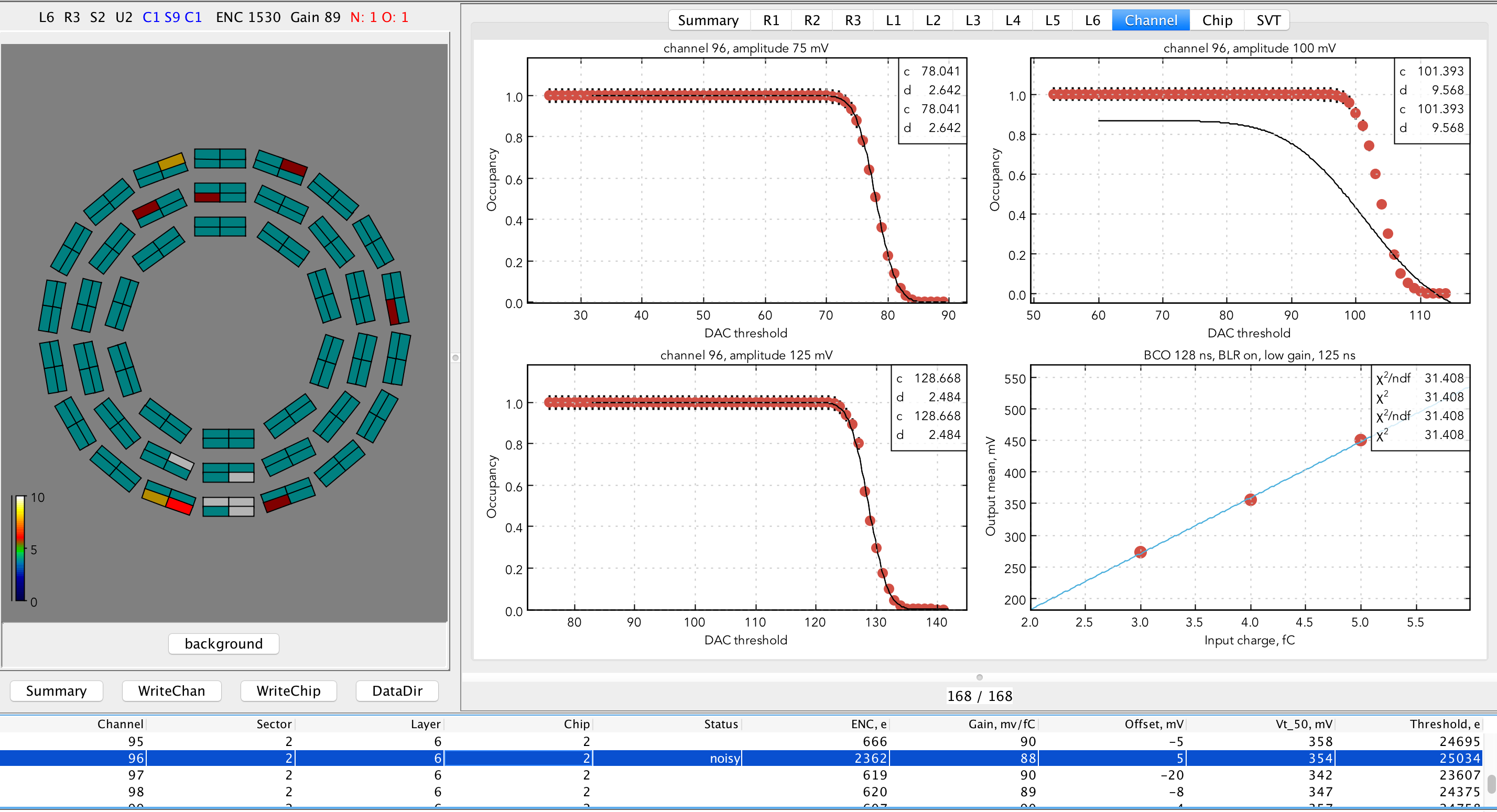
Fig. 20 Calibration plots with failed fit of the threshold scan
In case of the dead channel, the threshold occupancy plots would have only zero occupancy data, and the response function plot would be empty (Fig. 21).
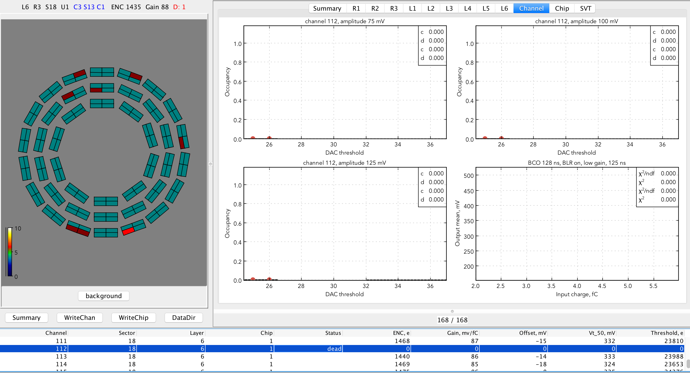
Fig. 21 Channel calibration plots for a dead channel
SVT calibration data are stored in the CCDB. The ASCII tables with constants are written from the GUI by pressing “WriteChan”, and “”WriteChip”. Channel calibration table has columns corresponding to sector, layer, chip number (1 – U1/U3, 2 – U2/U4), channel, channel status (0 – good, 1 – noisy, 2 – open, 3 – dead, 4 - masked), ENC (electrons), gain (mV/fC), offset (mV), Vt50 (mV), and threshold in electrons (Fig. 22). There are 21504 rows in the channel calibration table. ENC and gain are calculated using calibration amplitude equal to 100 DAC.

Fig. 22 Channel calibration table
Chip calibration table has columns corresponding to sector, layer, chip number (1 – U1/U3, 2 – U2/U4), mean ENC (electrons), ENC RMS, mean gain (mV/fC), gain RMS, mean offset (mV), offset RMS, mean Vt50 (mV), Vt50 RMS, threshold RMS (electrons), chip gain (0 – low, 1 – high), BLR mode (0 – off, 1 – on), BCO time (ns), shaper time (ns), 8 ADC thresholds in DAC (Fig. 23). There are 168 rows in the chip calibration table.
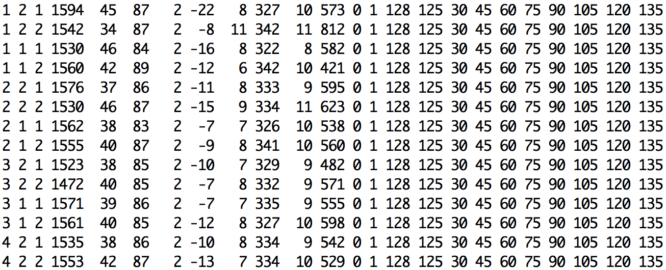
Fig. 23 Chip calibration table
To enter the SVT calibration tables into CCDB the following commands are entered (Fig. 24):
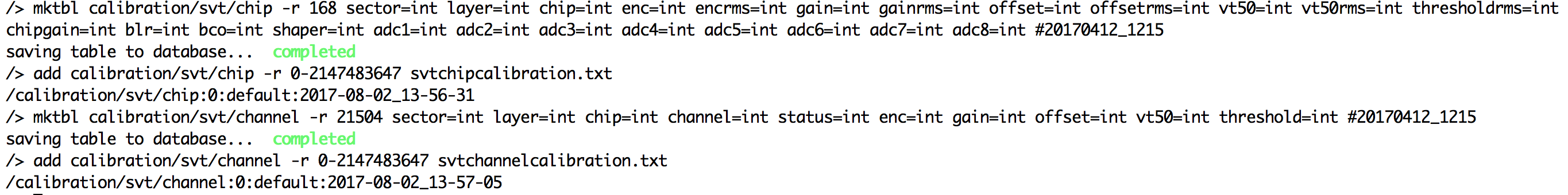
Fig. 24 Entering the calibration tables to CCDB
The channel table in the CCDB is shown in Fig. 25.
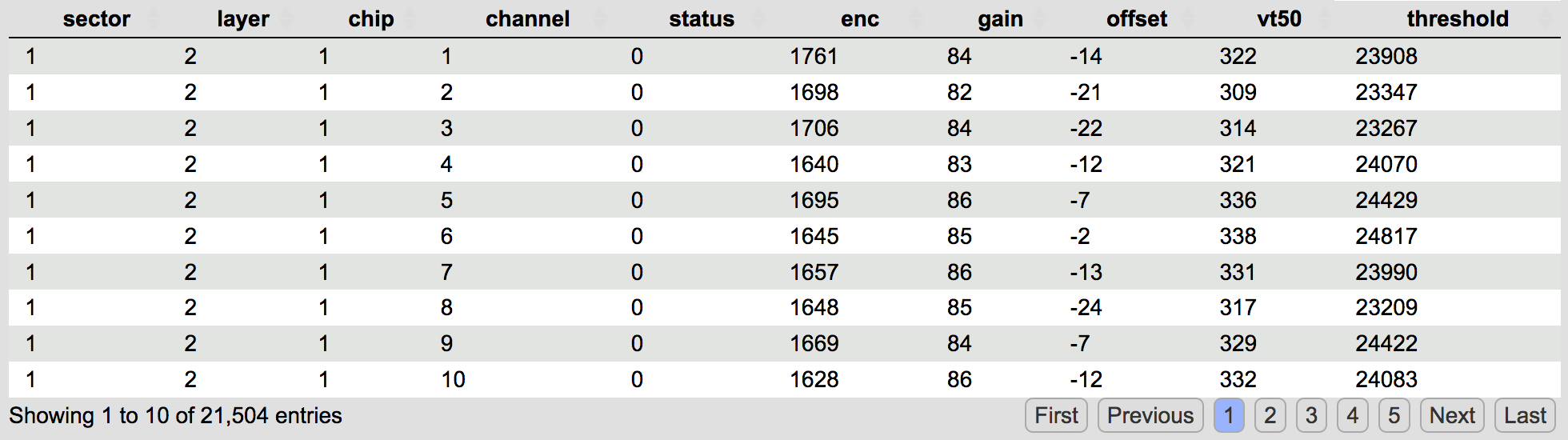
Fig. 25 SVT channel calibration table in CCDB
The chip table in the CCDB is shown in Fig. 26.

Fig. 26 SVT chip calibration table in CCDB